Does Hack Rf Have Hardware Id?
Like every open source hardware visitor, we've seen clones of our products for sale on the Cyberspace. These clones arguably provide a valuable service to the community, making our designs more than widely available and at a price more people can afford. Withal, they also take negative effects such as an increase on our technical back up burden without a corresponding increment in revenue to pay our staff. When the quality of a clone is poor information technology may also dethrone the reputation of our products.
Our most oftentimes cloned production is HackRF One. While we have every reason to believe that some of the HackRF clones on the market place are perfectly functional, we've seen users struggle to get others to piece of work at all. Some of the clones have been completely dead on arrival or have had other hardware problems. In general, it seems that few of the clones have been tested past their manufacturers. This can exist particularly problematic if returns are non accepted.
We recently decided for the first fourth dimension to order a HackRF clone and test it to run across how well information technology performs. Nosotros chose this detail clone considering it has an updated design claimed to improve upon our ain design. We're interested in potential improvements we can make to our ain product, and it seemed that the easiest way to test these modifications would be to simply purchase the modified clone.
When we plugged the clone in, it appeared to function normally. It had shipped with firmware congenital from the Havoc repository. This makes some sense as the seller too sells a clone of Jared Boone's excellent PortaPack. If someone were to purchase both products, the PortaPack would work out-of-the-box with the installed firmware. Nosotros weren't testing with a PortaPack, so we did some initial tests with the installed firmware and and so replaced the firmware with a fresh build from our repository.
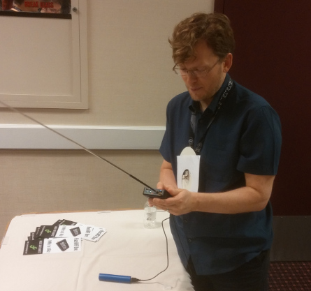
After confirming bones functionality, we executed a sweep to test the maximum output power across the unabridged 6 GHz frequency range. Nosotros did this past scripting a sequence of hackrf_transfer transmit commands while the device was connected to a spectrum analyzer. The results were troubling.
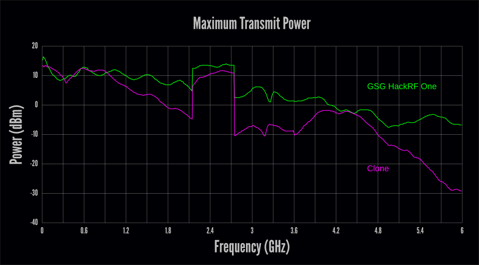
The clone conspicuously suffered from performance issues higher up 1 GHz, generally getting worse at higher frequencies. At half-dozen GHz, this culminated in a whopping 22 dB of loss compared to the GSG HackRF I. (That means that the GSG device produced more than 150 times the output ability of the clone.)
It is important to realize that we tested only ane sample clone, so our results may non exist representative of the average performance of this model. On the other hand, although these results are compared to a single Neat Scott Gadgets HackRF One, we know that every GSG HackRF One is factory-tested to ensure that it meets our operation standards.
Next we tested the receive operation by using QSpectrumAnalyzer with the hackrf_sweep backend. We set the gain to 40 in QSpectrumAnalyzer which results in moderate values for the 2 internal RX gain stages but leaves the RF amplifier off. We connected the device to a bespeak generator producing a -30 dBm signal, slowly swept across the 6 GHz frequency range.
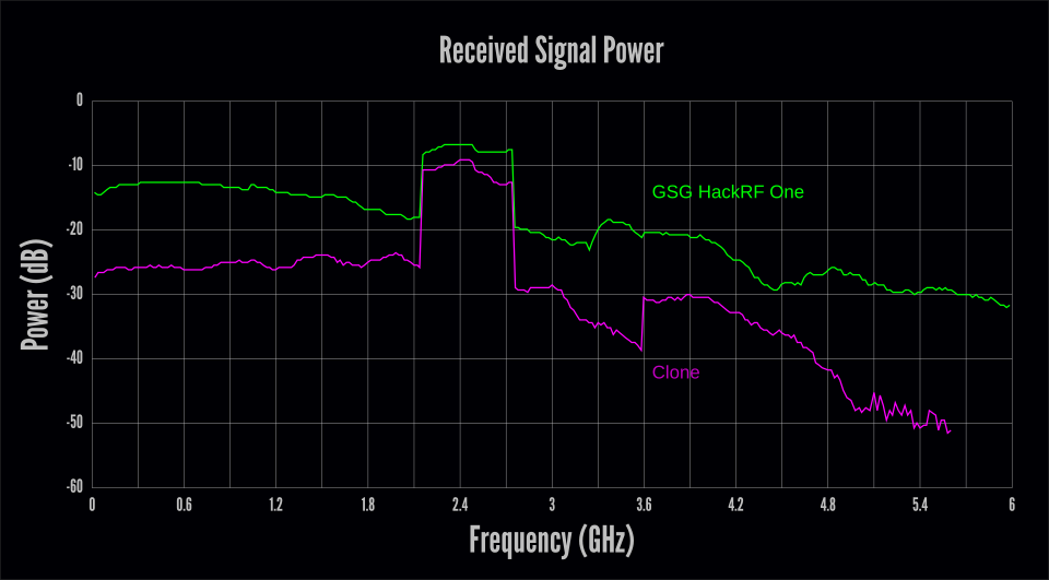
The receive results were even worse than the transmit results. While the transmit test indicated functioning issues above one GHz, the receive test revealed bug across the unabridged frequency range. Above 5 GHz the received signal was buried in the dissonance floor, completely undetectable above five.6 GHz by QSpectrumAnalyzer with these settings. Note that the RF amplifier was disabled in the receive examination simply had been enabled in the transmit test.
At this bespeak we ran the clone through our factory exam procedure which, in agreement with the previous results, indicated multiple failures at both high and depression frequencies. This unit would not have passed our quality command.
Nosotros suspected that in that location may have been multiple reasons for these failures including issues with the design changes likewise every bit manufacturing defects. We didn't think it would be worth our time trying to isolate every trouble, but we did want to explore the effect of the nigh interesting modification to the design, a protection circuit purported to reduce susceptibility to harm in the RF front end end. The simplest way we thought of to test the performance impact of the modification was to remove it and retest the lath without the protection circuit in place.
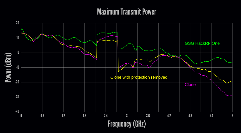
A echo of the transmit test immune us to see how the protection excursion afflicted signal power at various frequencies. As we suspected, a significant portion of the loss at college frequencies was eliminated by removing the protection excursion. However, the average performance beneath 5 GHz was little changed, suggesting the presence of additional design or manufacturing flaws.
10 dB of loss at the high stop of the frequency range seems to us like a steep price to pay for some protection. HackRF Ane is already weakest at 6 GHz. If it were that much weaker, I'm not sure nosotros would be comfortable advertising 6 GHz capability.
We are interested in increasing the robustness of the HackRF front end terminate, but whatsoever changes we brand would need to maintain acceptable RF performance. Possibly some functioning loss in exchange for protection could be adequate if the protection were proven by test results. We have not seen any exam results for the effectiveness of the protection circuit on this HackRF clone, but it is clear from our tests that its effect on RF performance is not acceptable.
HackRF One has an RX input rating of -5dBm. To the best of our noesis, it is not possible to damage the front terminate without exceeding this level. We are working on identifying reproducible scenarios that tin crusade damage to the RF forepart then that we tin can set upward reliable and repeatable tests for forepart finish protection. This will enable us to test changes that might increase the RX input rating and reduce the chance of harm in the field.
We're able to keep supporting and developing HackRF Ane and other tools thanks to the many people who choose to buy genuine Great Scott Gadgets products. Every GSG HackRF Ane is tested for quality at the mill. We provide technical support for our products, and we accept returns of faulty units through our authorized resellers.
Hopefully some of the HackRF clones on the market perform better than the one we tested. The best fashion we know of to ensure commitment of a working HackRF is to purchase it from one of our resellers. If you've bought hardware from us for this reason or just considering you want to support our ongoing open source development, cheers very much!
Thank you to everyone who has been a office of the GSG project mailing lists. Nosotros at Great Scott Gadgets appreciate all of the conversations and friendships that have been forged on these lists. Over the last few years nosotros have non given our project-specific mailing lists the attention they deserve; instead nosotros accept been focusing our efforts on Discord and GitHub. As such, nosotros will be disabling all the mailing lists except for GSG-announce. Links to the mailing list athenaeum for Ubertooth, Chiliad Stick Ane, GreatFET I, and HackRF will all remain available on their private product pages. Current links to the archives are here:
- Ubertooth-general
- YARDStick
- GreatFET
- HackRF-dev
We promise to run across all of you on Discord and GitHub shortly!
In this interview, Michael Ossmann visits Adafruit in New York and chats with Limor "Ladyada" Fried nigh GreatFET and HackRF. The two talk nigh what GreatFET neighbours are, how to design GreatFET neighbours, and Mike demonstrates how to use a wiggler to carve up neighbours from a GreatFET. This is followed up with a brusque discussion on HackRF and Portapack and how they piece of work together.
Around the first of the year our contract manufacturer contacted u.s.a. about an urgent problem with HackRF One product. They'd had to end product considering units coming off the line were declining at a high rate. This was quite a surprise because HackRF Ane is a mature product that has been manufactured regularly for a few years. I continued to find surprises equally I went through the procedure of troubleshooting the problem, and I thought it made a fascinating tale that would be worth sharing.
The reported failure was an disability to write firmware to the flash memory on the lath. Our attention quickly turned to the wink scrap itself because it was the i thing that had changed since the previous production. The original flash flake in the design had been discontinued, so nosotros had selected a replacement from the same manufacturer. Although we had been careful to test the new chip prior to product, it seemed that somehow the change had resulted in a high failure charge per unit.

Had we overlooked a failure way considering we had tested too small a quantity of the new flash chips? Had the sample parts we tested been unlike than the parts used in the production? Nosotros quickly ordered parts from multiple sources and had our contract manufacturer send us some of their parts and new boards for testing. Nosotros began testing parts as soon as they arrived at our lab, but even subsequently days of testing samples from various sources we were unable to reproduce the failures reported by the contract manufacturer.
At one point I thought I managed to reproduce the failure on one of the new boards, but it only happened well-nigh 3% of the time. This failure happened regardless of which flash fleck was used, and it was easy to work around by retrying. If it happened on the production line it probably wouldn't fifty-fifty be noticed considering it was indistinguishable from a simple user error such as a poor cable connection or a missed button press. Eventually I determined that this low probability failure mode was something that affected older boards as well. Information technology is something we might be able to fix, but information technology is a low priority. Information technology certainly wasn't the same failure mode that had stopped product.
It seemed that the new flash chip acquired no problems, just so what could exist causing the failures at the factory? We had them ship us more sample boards, specifically requesting boards that had exhibited failures. They had intended to send us those in the start shipment but accidentally left them out of the parcel. Because the flash flake was and so strongly suspected at the fourth dimension, we'd all thought that nosotros'd be able to reproduce the failure with one or more of the many fries in that packet anyway. One thing that had fabricated information technology difficult for them to know which boards to ship was that whatever board that passed testing in one case would never fail again. For this reason they had deemed it more of import to send us fresh, untested boards than boards that had failed and later passed.
When the second batch of boards from the contract manufacturer arrived, we immediately started testing them. We weren't able to reproduce the failure on the first board in the shipment. We weren't able to reproduce the failure on the 2d board either! Fortunately the next three boards exhibited the failure, and nosotros were finally able to notice the trouble in our lab. I isolated the failure to something that happened earlier the bodily programming of the flash, so I was able to develop a exam process that left the wink empty, avoiding the scenario in which a board that passed once would never fail again. Even later on being able to reliably reproduce the failure, it took several days of troubleshooting to fully sympathize the problem. Information technology was a frustrating process at the time, but the root cause turned out to be quite an interesting bug.
Although the initial symptom was a failure to plan wink, the means of programming wink on a new board is actually a multi-footstep process. First the HackRF Ane is booted in Device Firmware Upgrade (DFU) mode. This is done by holding downward the DFU push button while powering on or resetting the board. In DFU mode, the HackRF'due south microcontroller executes a DFU bootloader function stored in ROM. The host figurer speaks to the bootloader over USB and loads HackRF firmware into RAM. Then the bootloader executes this firmware which appears as a new USB device to the host. Finally the host uses a function of the firmware running in RAM to load some other version of the firmware over USB and onto the wink fleck.
I found that the failure happened at the step in which the DFU bootloader launches our firmware from RAM. The load of firmware over USB into RAM appeared to piece of work, but then the DFU bootloader dropped off the bus and the USB host was unable to re-enumerate the device. I probed the board with a voltmeter and oscilloscope, but virtually everything looked equally expected. There was a adequately significant voltage glitch on the microcontroller's power supply (VCC), simply a probe of a known practiced board from a previous production revealed a similar glitch. I made a note of it as something to investigate in the future, merely information technology didn't seem to exist anything new.
I continued a Black Magic Probe and investigated the country of the microcontroller before and after the failure. Before the failure, the program counter pointed to the ROM region that contains the DFU bootloader. After the failure, the plan counter still pointed to the ROM region, suggesting that command may never have passed to the HackRF firmware. I inspected RAM after the failure and found that our firmware was in the right place only that the outset sixteen bytes had been replaced by 0xff. Information technology made sense that the bootloader would not effort to execute our code because it is supposed to perform an integrity check over the kickoff few bytes. Since those bytes were corrupted, the bootloader should have refused to leap to our lawmaking.
I monitored the USB communication to see if the firmware prototype was corrupted before being delivered to the bootloader, just the start xvi bytes were right in transit. Naught looked out of the ordinary on USB except that there was no indication that the HackRF firmware had started up. Afterwards the bootloader accepted the firmware epitome, information technology dropped off the double-decker, and and then the bus was silent.
Equally my testing progressed, I began to notice a curious thing, and our contract manufacturer reported the very same observation: The RF LED on the board sometimes was dimly illuminated in DFU mode and sometimes was completely off. Whenever it was off, the failure would occur; whenever it was dimly on, the board would pass testing. This inconsistency in the state of the RF LED is something that nosotros had observed for years. I had never given information technology much thought but assumed it may have been caused by some known bugs in reset functions of the microcontroller. Of a sudden this beliefs was very interesting because it was strongly correlated with the new failure! What causes the RF LED to sometimes be dimly on at kicking fourth dimension? What causes the new failure? Could they be caused by the same thing?
I took a look at the schematic which reminded me that the RF LED is not connected to a General-Purpose Input/Output (GPIO) pin of the microcontroller. Instead it directly indicates the state of the power supply (VAA) for the RF department of the board. When VAA is low (below about one.5 Volts), the RF LED is off. When VAA is at or nigh three.3 Volts (the same voltage as VCC), the RF LED should be fully on. If the RF LED is dimly on, VAA must be at approximately two Volts, the forward voltage of the LED. This isn't enough voltage to power the chips in the RF department, but it is enough to dimly illuminate the LED.

VAA is derived from VCC simply is controlled by a MOSFET which switches VAA on and off. At boot time, the MOSFET should be switched off, but somehow some current can leak into VAA. I wasn't certain if this leakage was due to the land of the GPIO indicate that controls the MOSFET (!VAA_ENABLE) or if it could be from ane of several digital control signals that extend from the VCC power domain into the VAA power domain. I probed all of those signals on both a good lath and a declining lath merely didn't find any pregnant differences. It wasn't clear why VAA was sometimes partially charged at outset-up, and I couldn't find whatsoever indication of what might be unlike between a good lath and a bad board.
One matter that was clear was that the RF LED was e'er dimly illuminated immediately after a failure. If I reset a lath into DFU mode using the reset push subsequently a failure, the RF LED would remain dimly lit, and the failure would be avoided on the second endeavor. If I reset a board into DFU mode by removing and restoring power instead of using the reset button, the RF LED country became unpredictable. The procedural workaround of retrying with the reset push button would take been sufficient to proceed with manufacturing except that we were nervous about shipping boards that would give cease users trouble if they need to recover from a load of faulty firmware. It might exist a support nightmare to have units in the field that do non provide a reliable means of restoring firmware. Nosotros certainly wanted to at least empathize the root crusade of the problem before agreeing to ship units that would require users to follow a procedural workaround.
Meanwhile I had removed a large number of components from one of the failing boards. I had started this process after determining that the flash chip was not causing the problem. In order to prove this without a doubt, I entirely removed the flash chip from a failing lath and was still able to reproduce the failure. I had continued removing components that seemed unrelated to the failure but to evidence to myself that they were non involved. When investigating the correlation with VAA, I tried removing the MOSFET (Q3) and constitute that the failure did not occur when Q3 was absent! I likewise found that removal of the ferrite filter (FB2) on VAA or the capacitor (C105) would preclude the failure. Whenever whatever of these three components was removed, the failure could be avoided. I tried cut the trace (P36) that connects the VAA MOSFET and filter to the residue of VAA. Even without any connection to the load, I could foreclose the failure past removing whatever of those 3 components and induce the failure by restoring all three. Perhaps the charging of VAA was not just correlated with the failure simply was somehow the cause of the failure!
This prompted me to spend some time investigating VAA, VCC, and !VAA_ENABLE more thoroughly. I wanted to fully sympathise why VAA was sometimes partially charged and why the failure just happened when it was uncharged. I used an oscilloscope to probe all three signals simultaneously, and I tried triggering on changes to any of the three. Earlier long I found that triggering on !VAA_ENABLE was most fruitful. It turned out that !VAA_ENABLE was being pulled low very briefly at the approximate fourth dimension of the failure. This signal was meant to remain loftier until the HackRF firmware pulls it depression to switch on VAA. Why was the DFU bootloader toggling this pin before executing our firmware?
Had something inverse in the DFU bootloader ROM? I used the Blackness Magic Probe to dump the ROM from ane of the new microcontrollers, but it was the same as the ROM on older ones. I even swapped the microcontrollers of a adept lath and a bad lath; the bad lath continued to fail even with a known good microcontroller, and the good board never exhibited a problem with the new microcontroller installed. I investigated the behavior of !VAA_ENABLE on a good board and found that a like glitch happened prior to the point in time at which the HackRF firmware pulls it low. I didn't understand what was different betwixt a practiced board and a bad board, but it seemed that this behavior of !VAA_ENABLE was somehow responsible for the failure.
The transient change in !VAA_ENABLE caused a small rise in VAA and a brief, very pocket-size dip in VCC. It didn't wait similar this dip would exist enough to cause a trouble on the microcontroller, but, on the assumption that information technology might, I experimented with ways to avert affecting VCC every bit much. I found that a reliable hardware workaround was to install a ane kΩ resistor betwixt VAA and VCC. This caused VAA to ever be partially charged prior to !VAA_ENABLE being toggled, and information technology prevented the failure. Information technology wasn't a very attractive workaround because at that place isn't a good place to install the resistor without changing the layout of the board, simply we were able to confirm that information technology was effective on all boards that suffered from the failure.
Trying to decide why the DFU bootloader might toggle !VAA_ENABLE, I looked at the documented functions available on the microcontroller'southward pin that is used for that betoken. Its default function is GPIO, but it has a secondary office as a part of an external retentivity interface. Was information technology possible that the DFU bootloader was activating the external retentivity interface when writing the firmware to internal RAM? Had I made a terrible mistake when I selected that pin years ago, unaware of this bootloader behavior?
Unfortunately the DFU bootloader is a ROM office provided by the microcontroller vendor, so we don't have source code for it. I did some cursory opposite engineering of the ROM only couldn't detect any indication that it possesses the capability of activating the external memory interface. I tried using the Blackness Magic Probe to single step through instructions, only it wasn't fast enough to avert USB timeouts while unmarried stepping. I fix a watchpoint on a annals that should exist set when powering up the external retentivity interface, but it never seemed to happen. Then I tried setting a watchpoint on the annals that sets the pin function, and suddenly something very surprising was revealed to me. The first time the pin role was set was in my own code executing from RAM. The bootloader was actually executing my firmware fifty-fifty when the failure occurred!
After a brief moment of disbelief I realized what was going on. The reason I had idea that my firmware never ran was that the plan counter pointed to ROM both before and after the failure, but that wasn't considering my lawmaking never executed. A ROM function was running after the failure because the microcontroller was beingness reset during the failure. The failure was occurring during execution of my own lawmaking and was likely something I could set up in software! Function of the reason I had misinterpreted this behavior was that I had been thinking about the bootloader as "the DFU bootloader", but information technology is really a unified bootloader that supports several different boot methods. Fifty-fifty when booting to wink retentivity, the default boot option for HackRF One, the get-go code executed past the microcontroller is the bootloader in ROM which later on passes control to the firmware in wink. You don't hold downward the DFU push button to cause the bootloader to execute, you lot hold down the button to instruct the bootloader to load code from USB DFU instead of wink.
All of a sudden I understood that the memory corruption was something that happened equally an upshot of the failure; information technology wasn't part of the cause. I also understood why the failure did non seem to occur afterwards a board passed testing once. During the test, firmware is written to flash. If the failure occurs at whatsoever time thereafter, the microcontroller resets and boots from flash, behaving similarly to how information technology would behave if it had correctly executed code that had been loaded via USB into RAM. The reason the board was stuck in a ROM function after a failure on a board with empty flash was simply that the bootloader was unable to detect valid firmware in wink after reset.
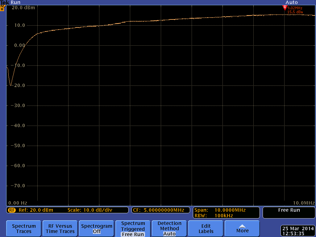
Information technology seemed clear that the microcontroller must be experiencing a reset due to a voltage glitch on VCC, but the glitch that I had observed on failing boards seemed as well small to have acquired a reset. When I realized this, I took some more than measurements of VCC and zoomed out to a wider view on the oscilloscope. There was a second glitch! The second glitch in VCC was much bigger than the outset. It was also caused by !VAA_ENABLE being pulled low, just this time it was held depression long enough to have a much larger effect on VCC. In fact, this was the same glitch that I had previously observed on known practiced boards. I then determined that the first glitch was caused by a modest bug in the way our firmware configured the GPIO pin. The 2nd glitch was caused by the deliberate activation of !VAA_ENABLE.
 glitch caused by rapid charging of VAA (orange) when !VAA_ENABLE (yellow) is pulled low")
When a good board starts upward, it pulls !VAA_ENABLE low to activate the MOSFET that switches on VAA. At this time, quite a scrap of electric current gets dumped into the capacitor (C105) in a curt amount of time. This is a perfect recipe for causing a brief drop in VCC. I knew about this potential trouble when I designed the excursion, just I guess I didn't carefully measure it at the time. Information technology never seemed to crusade a problem on my prototypes.
When a bad board starts up, the exact same thing happens except the voltage drop of VCC is simply a little bit deeper. This causes a microcontroller reset, resulting in !VAA_ENABLE existence pulled high over again. During this brief glitch VAA becomes partially charged, which is why the RF LED is dimly lit subsequently a failure. If VAA is partially charged before !VAA_ENABLE is pulled low, less current is required to fully charge it, and then the voltage glitch on VCC isn't deep plenty to cause a reset.
At this indicate I figured out that the reason the land of the RF LED is unpredictable after power is practical is that it depends on how long power has been removed from the board. If y'all unplug a board with VAA at least partially charged but so plug information technology dorsum in within ii seconds, VAA will still exist partially charged. If you lot go out it disconnected from ability for at least five seconds, VAA will be thoroughly discharged and the RF LED will be off subsequently plugging information technology back in.
This sort of voltage glitch is something hardware hackers innovate at times as a fault injection attack to cause microcontrollers to misbehave in useful ways. In this case, my microcontroller was glitching itself, which was not a practiced thing! Fortunately I was able to prepare the problem by rapidly toggling !VAA_ENABLE many times, causing VAA to accuse more than slowly and avoiding the VCC glitch.
 glitch avoided by rapid toggling of !VAA_ENABLE (yellow) to slowly charge of VAA (orange)")
I'm all the same not entirely certain why boards from the new production seem to be more sensitive to this failure than older boards, but I have a guess. My guess is that a certain pct of units have always suffered from this trouble but that they accept gone undetected. The people programming the boards in previous productions may have figured out on their own that they could relieve fourth dimension by using the reset push button instead of unplugging a board and plugging it dorsum in to try once again. If they did then, they would accept had a very high success rate on second attempts even when programming failed the first time. If a new employee or two were doing the programming this fourth dimension, they may have followed their instructions more than advisedly, removing failing boards from power earlier re-testing them.
Even if my gauge is incorrect, it seems that my blueprint was always very shut to having this trouble. Known skillful boards suffered from less of a glitch, merely they still experienced a glitch that was close to the threshold that would cause a reset. Information technology is entirely possible that subtle changes in the characteristics of capacitors or other components on the board could cause this glitch to be greater or smaller from 1 batch to the side by side.
Once a HackRF One has had its flash programmed, the problem is very likely to become undetected forever. Information technology turns out that this glitch can happen even when a board is booted from flash, not just when starting it upward in DFU mode. When starting from wink, however, a glitch-induced reset results in another boot from wink, this time with VAA charged up a niggling scrap more than. After one or ii resets that happen in the blink of an eye, it starts upward usually without a glitch. Unless you know what to look for, it is quite unlikely that y'all would e'er detect the fault.
Because of this and the fact that we didn't have a way to distinguish between firmware running from flash and RAM, the failure was hard for us to reproduce and observe reliably before we understood it. Some other thing that complicated troubleshooting was that I was very focused on looking for something that had changed since the previous production. Information technology turned out that the voltage glitch was only subtly worse than it was on the older boards I tested, and then I overlooked it as a possible cause. I don't know that it was necessarily wrong to have this focus, but I might have establish the root cause faster had I concentrated more on understanding the problem and less on trying to discover things that had changed.
In the cease I found that information technology was my own hardware pattern that acquired the problem. It was another example of something Jared Boone oftentimes says. I call it ShareBrained's Razor: "If your projection is broken, information technology is probably your fault.". It isn't your compiler or your components or your tools; it is something you did yourself.
Thank you to everyone who helped with this troubleshooting process, peculiarly the entire GSG squad, Etonnet, and Kate Temkin. Also thank you to the pioneers of antibiotics without which I would take had a significantly more difficult recovery from the bronchitis that afflicted me during this effort!
Today we are excited to denote the official release of ANT700, our new 300—1100 MHz scope antenna. Because this general purpose antenna was designed with Yard Stick One users in mind, it has a slim and lightweight form factor that works well with smaller devices. Information technology has an SMA male person connector to attach to your device of choice (including HackRF One) and tin can be extended from 9.v cm to 24.5 cm.
We started distributing ANT700 last month, and it is already available for buy from six of our authorized resellers on four continents. To detect out where you can purchase yours, please visit the product folio.
In this video of my presentation at ToorCon 2015, I demonstrate how helpful it tin can exist to utilise a combination of both SDR and not-SDR tools for reverse applied science wireless systems. I use both HackRF Ane and K Stick One to opposite engineer a wireless cabinet lock.
download video
lawmaking from the presentation
Jared Boone of ShareBrained Technology gave demonstrations of his new PortaPack H1 at the DEF CON 23 Demo Lab. I joined him at his table to assistance talk with people about the add-on for HackRF One.
PortaPack H1 turns HackRF One into a portable SDR platform. With an LCD, navigation control, and audio input and output, the device tin can be used as a handheld spectrum analyzer and tin implement a wide variety of useful radio functions. A microSD slot on the PortaPack can exist used for waveform or firmware storage, and a money cell keeps the existent-time clock and a pocket-sized amount of configuration RAM going while the device is turned off.

Of course, the hardware designs and firmware for PortaPack H1 are published under an open up source license. Jared has done an amazing job of implementing SDR functions for PortaPack that run entirely on HackRF One's ARM Cortex-M4 microcontroller.
To use PortaPack H1, you'll demand a HackRF One, and you'll probably desire a USB battery pack to brand information technology a fully portable solution. Another popular addition is the beautiful milled Aluminum enclosure for PortaPack. Jared provides a ShareBrained Technology guitar pick with every PortaPack H1. It is the perfect tool for opening your HackRF One's injection molded plastic enclosure prior to PortaPack installation.
In that location was a wonderful moment at the Demo Lab when Jared tuned his PortaPack to a frequency being used by Ang Cui at a nearby table. Jared's PortaPack was plugged in to a small speaker, and then we could all listen to the AM radio transmission originating from a printer at Ang's table. The printer was physically unmodified simply was running malicious software that transmitted radio signals with a funtenna! For more information about Ang's implementation, visit funtenna.org.
Over the next several days, thousands of hackers volition get together at the Chaos Communication Camp in Germany. An electronic badge for the result is being prepared, and it is based on my design for HackRF One!
At DEF CON over the weekend, I was fortunate to be able to meet upward with Ray, ane of the members of the Munich CCC grouping responsible for the rad1o badge. Ray was wearing one of the prototype units, so I was able to take a close look.

The design is a variation of HackRF 1. It includes a pocket-sized LCD and an audio interface, so it is a fleck like having a HackRF I plus a PortaPack H1 on a single board. A slim, rechargeable LiPo bombardment is mounted on the back. The visual design of the PCB looks like a traditional AM/FM radio receiver complete with an antenna (which is not the actual RF antenna) and a dial (which is non really a dial).
In that location are some design modifications, especially in the RF department, that seemed strange to me at first. The reason for many of these changes is that the rad1o squad was able to get certain chip vendors to agree to sponsor the bluecoat by altruistic parts. By redesigning effectually donated components they were able to reduce the price to a pocket-sized fraction of the price of manufacturing HackRF 1, making it possible to build the rad1o badge for several thousand campers.
The firmware for rad1o is derived from HackRF One firmware but is in a divide repository. Because of the LCD and other differences betwixt the ii hardware designs, they are not firmware-uniform. When using rad1o as a USB peripheral, it is fully supported past existing software that supports HackRF One. Future rad1o firmware volition use a USB product ID of 0xCC15 assigned from the Openmoko pool, but the aircraft firmware will infringe HackRF One'south product ID. This will ensure that whatever existing software for HackRF One will work with rad1o during camp. The new product ID (0xCC15) is already supported in libhackrf release 2015.07.2, so it should be piece of cake for people to update to it in the about future.
If you are new to Software Defined Radio and are looking forrad to using the badge every bit a way to get started with SDR, I recommend starting with my video series. You might want to download the videos before leaving for army camp. Also take a expect at Getting Started with HackRF and GNU Radio and the recommended software for rad1o. If yous plan to do firmware or hardware hacking, be sure to clone the rad1o repositories. For examples of Digital Bespeak Processing (DSP) on the LPC43xx, I suggest studying Jared Boone's firmware for PortaPack H1. Besides check out the video of Jared's Software-Defined Radio Signal Processing with a $5 Microcontroller at BSidesLV 2015.
As an open source hardware developer, it is extremely satisfying to come across folks start with my design and do something amazing like the rad1o bluecoat. I'm excited to be attending army camp for my first time ever, and I tin can't wait to see the projects people will come with!
Nosotros've decided to annunciate the fact that HackRF One operates all the fashion downwards to one MHz, non but to 10 MHz. This isn't a alter to the hardware blueprint; it is only an acquittance that the hardware has always worked at such low frequencies and that nosotros support performance downward to 1 MHz.
In fact, HackRF One can even function below 1 MHz, merely the operation drops considerably every bit the frequency decreases. The curve is reasonably flat down to about i MHz, so we consider that to be the lower limit for near uses.
Now that nosotros've seen consistent low frequency operation beyond multiple manufacturing runs, we're comfortable changing the official specification: HackRF One operates from one MHz to half dozen GHz. Attempt attaching a long wire antenna to listen to shortwave radio!
Although HackRF One has reasonable operation downwards to 1 MHz, it performs better at college frequencies. To get the best possible performance down to i MHz and lower, I recommend using an external upconverter/downconverter such every bit the excellent Ham It Up, open source hardware designed by Opendous.
0 Response to "Does Hack Rf Have Hardware Id?"
Post a Comment